Deep Dive: Blackwell B200
I’ve been going through blogs and papers regarding B200’s design and its tradeoffs. Here I will summarize what I’ve learned so far. B200 is NVIDIA’s datacenter Blackwell GPU: 148 SMs across two dies connected by NV-HBI, with 192 GB HBM3e at 8 TB/s and a 1000W TDP.
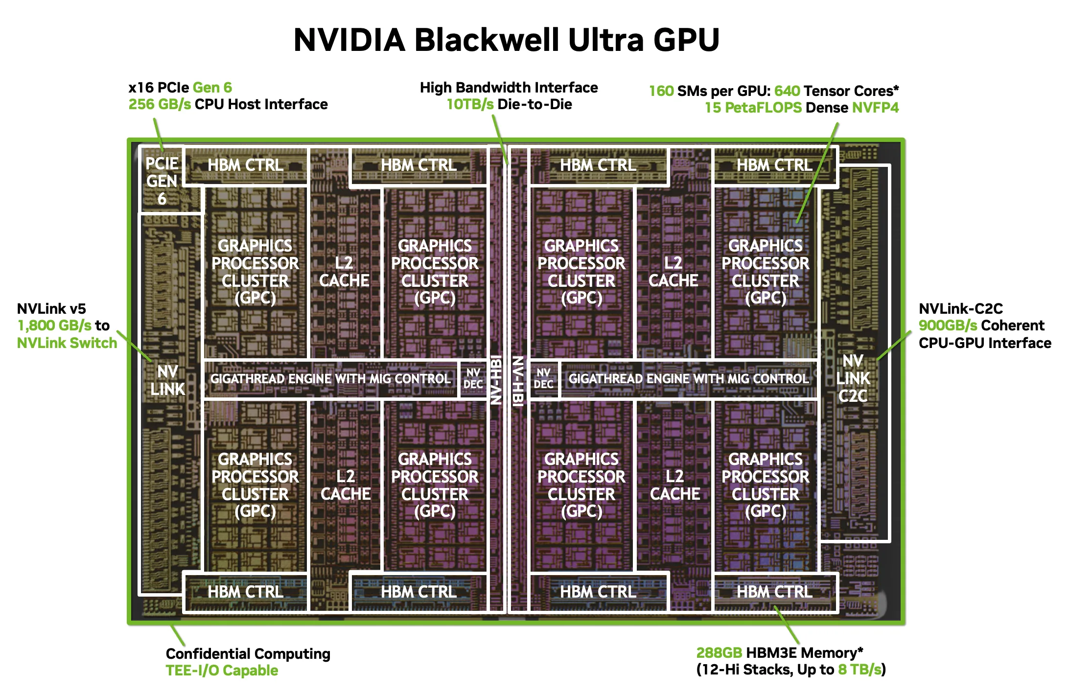
Quick comparison with the previous Hopper arch. B200 unifies the fp32 and int32 cores while introducing TMEM. It also introduces new 4bit Tensor Cores for int4/fp4.
| Component | Hopper (H100 SXM5) | Blackwell (B200) |
|---|---|---|
| SMs | 132 | 148 |
| GPCs | 8 | 8 (4 per die) |
| FP32/INT32 | 128 FP32 + 64 INT32 (separate) | 128 unified (FP32 or INT32 per cycle) |
| FP64 | 64 dedicated | ~64 dedicated per SM |
| Tensor Cores | 4 (4th-gen) | 4 (5th-gen) |
| TMEM | — | 256 KB |
| L1/SMEM per SM | 256 KB unified | 256 KB unified |
| L2 cache | 50 MB | ~126 MB |
| HBM | 80 GB @ 3.35 TB/s | 192 GB raw @ 8 TB/s |
| Native FP4/FP6 | No (FP8 only) | Yes |
Although Hopper has extra 64 int32 cores, they don’t raise its peak FFMA which remains around 128 FFMA/cycle/SM. This is the same for Blackwell as well.
Register Pressure and the TMEM Migration
Over the years Tensor Core instructions gained more direct access to SMEM but Blackwell moved accumulators into a new mem, TMEM.
| Architecture | Matrix A | Matrix B | Accumulator D | Key Instruction |
|---|---|---|---|---|
| Volta (2017) | Register | Register | Register | mma.sync |
| Ampere (2020) | Register | Register | Register | mma.sync |
| Hopper (2022) | SMEM / Register | SMEM | Register | wgmma.mma_async |
| Blackwell (2024) | TMEM / SMEM | SMEM | TMEM | tcgen05.mma |
TMEM (Tensor Memory) is a new on-SM scratchpad that’s private to the Tensor Cores. TMEM doesn’t support the typical load/store operations per thread. Typically, TMA moves data from global memory into shared memory, then tcgen05.mma reads operands from SMEM and writes the accumulator to TMEM. The only way to read it back into registers is tcgen05.ld.
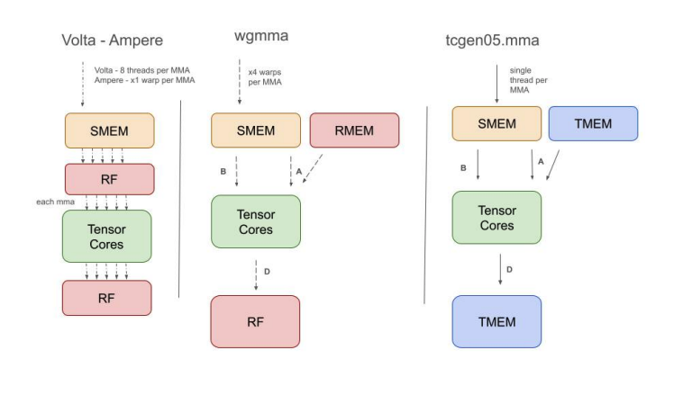
Each Tensor Core generation made MMA progressively less intrusive on the scalar pipeline by reducing the sync cost. On Volta and Ampere mma.sync is required for all 32 warp threads to participate but its latency can be hidden with independent overlapping instructions. Hopper’s wgmma.mma_async uses a warpgroup (128 threads) instead of a single warp and makes it asynchronous so the warpgroup could issue an MMA and then proceed to other work while it ran in the background.
Blackwell’s tcgen05.mma takes this to its logical endpoint. A single thread issues the MMA on behalf of the entire CTA. The other 127 threads never touch the MMA path, they’re free to issue TMA loads, manage barriers or compute addresses concurrently. This is “full decoupling”. The Tensor Cores are now independent coprocessors driven by one thread with its accumulator in TMEM and completely separate from the scalar register file.
Register Pressure
I compiled two CUTLASS tutorial GEMM kernels on the B200:
- Ampere path (
sgemm_sm80.cu): usesmma.syncwith a 128×64 tile, FP16 inputs and an FP16 accumulator held in registers. Compiled withnvcc -arch=sm_100(backward-compatible on B200). - Blackwell path (
01_mma_sm100.cu): usestcgen05.mmawith a 128×256 tile, FP16 inputs and an FP32 accumulator held in TMEM. Compiled withnvcc -arch=sm_100a(theavariant enablestcgen05/TMEM).
Both were compiled with -ptxas-options=-v which makes the PTX assembler print register allocation for every function.
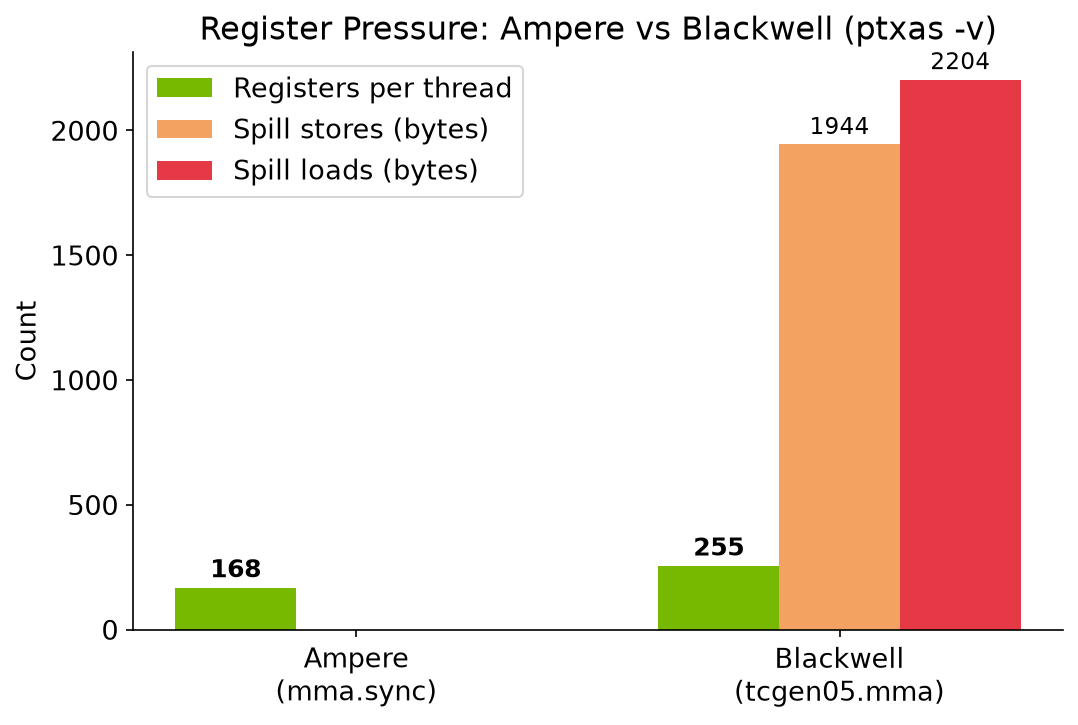
I observed that the Blackwell kernel hits the 255 register ceiling and spills to local memory. The question is, if TMEM removes the accumulator from the register file then why does it need more registers and not fewer?
Since NCU isn’t available on a RunPod cloud instance, I used kernel modification and SASS disassembly. I replaced the full epilogue with a minimal checksum epilogue that still consumed the TMEM accumulator. The resulting kernel used 61 registers with no spills while retaining the same eight static UTCHMMA instructions as the full kernel. I then disassembled the full kernel with cuobjdump –dump-sass and found 0 static LDL sites in the MMA mainloop and 547 in the epilogue. Together with the ptxas spill report, this shows that, in this kernel, peak register pressure and spilling arise when the TMEM accumulator is materialized into registers for the epilogue, rather than during the MMA mainloop.
The point of TMEM isn’t fewer registers in total. It’s to keep the compute phase’s registers free so the MMA pipeline stays fed. The epilogue can tolerate spills because it can be chunked but the compute phase can’t.
SFU Throughput
B200 Tensor Cores are enormously fast with 2.25 PFLOPS in FP16 and 9 PFLOPS in FP4. But attention isn’t just matmul. After QK^T you run softmax(QK^T / √d) which calls exp() on every element. The exp() function uses the special-function pipeline, through native instructions such as MUFU.EX2.
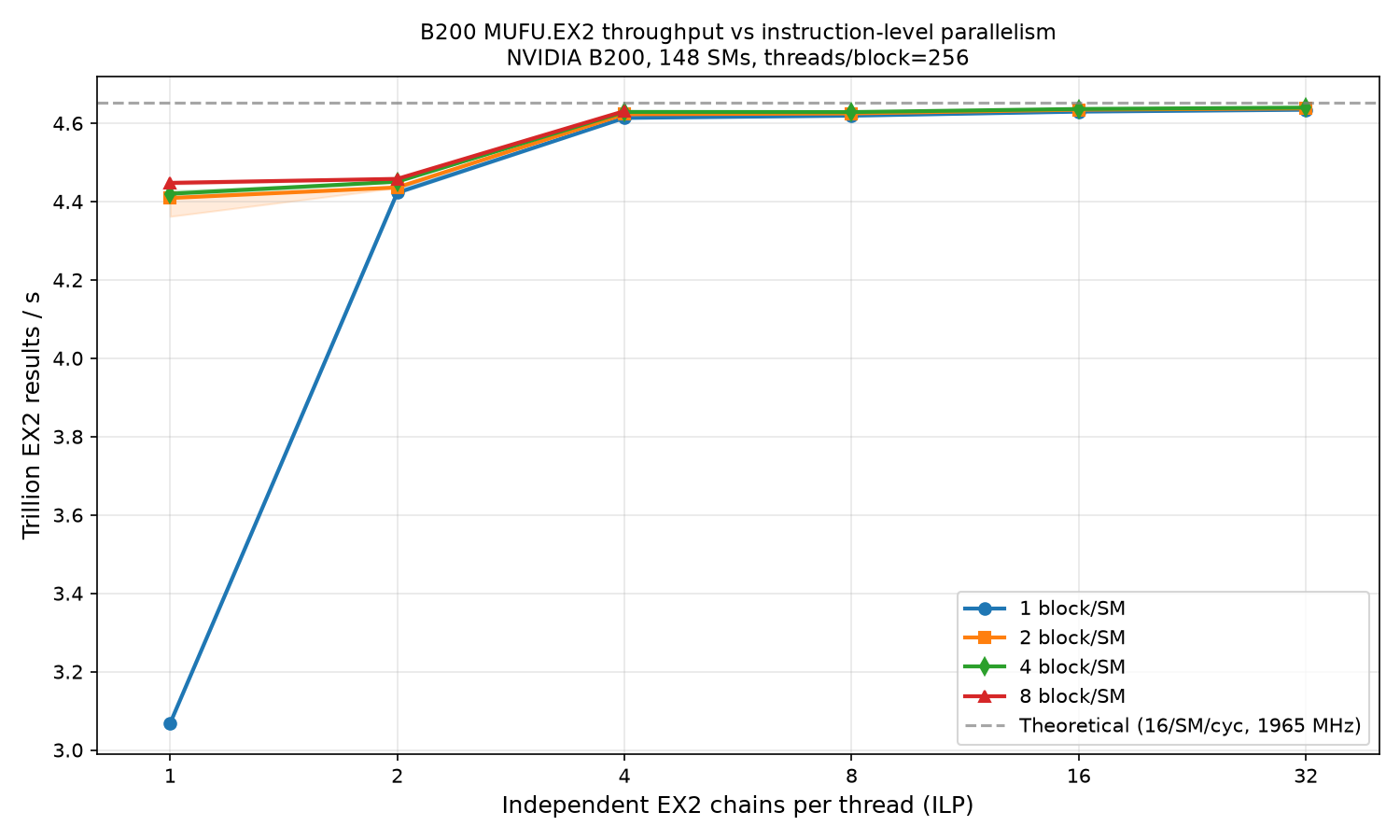
B200 can do 16 transcendental ops per SM per cycle while its Tensor Cores can do 8192 fp16 FLOPS. From Hopper to Blackwell, Tensor Core throughput increased substantially, but the documented transcendental throughput per SM remained unchanged. This widened the imbalance between matrix multiplication and operations such as exponentials.
To test this, I swept 1–32 independent instruction chains per thread, 128–512 threads per block, and multiple blocks per SM. I used ILP because a simple loop must wait for each result before issuing the next one. The ILP 8, 16 and 32 variants all remain near 4.65 trillion results/s, showing that the native MUFU.EX2 pipeline has reached its throughput ceiling. The seven measurements for the winning configuration ranged from 4.64898 to 4.64997 trillion results/s.
Cross-Die Memory Latency
The Architecture
B200 is two GPU dies in one package. Each die has its own L2 cache slice (~63MB) and its own HBM3e stacks (96GB). The two dies are connected by NV-HBI at 10 TB/s. An SM on die A can access die B’s L2 and HBM, but the request must traverse the NV-HBI interconnect. CUDA 13 exposes no CTA memory affinity API meaning you can’t tell the runtime “schedule this thread block near this data”.
L2: The Cross-Die Penalty is Visible
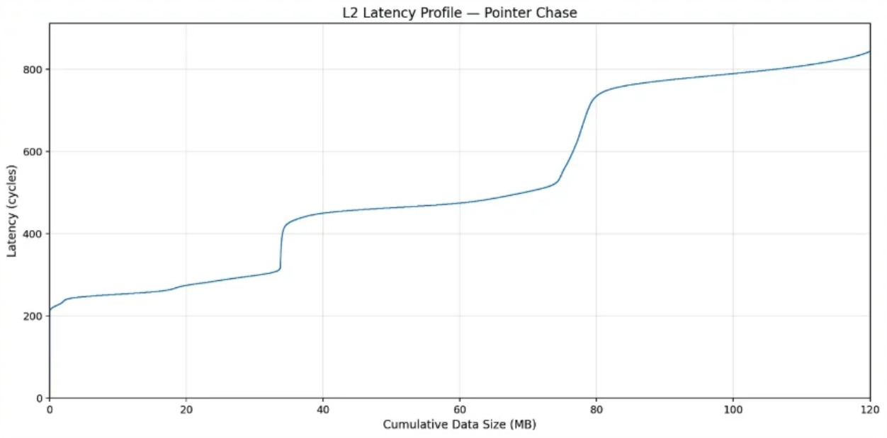
SemiAnalysis measured this directly. They ran an L2 sized pointer chase 126MB sized to fill L2. With all 148 SMs traversing the same shuffled chain and recording per load latency with clock64(). By comparing latency vectors between every SM pair they built a 148×148 distance matrix. Two clear clusters emerged which were separated by 300 cycles. SMs on the same die see similar L2 latency patterns while those on the different die see inverse patterns. Local L2 hit was 150 cycles and remote L2 hit (cross-die) was around 450 cycles. The 300 cycle NV-HBI crossing is a clean 3× signal at L2 depths.
HBM: The Penalty Disappears
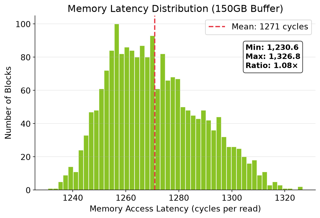
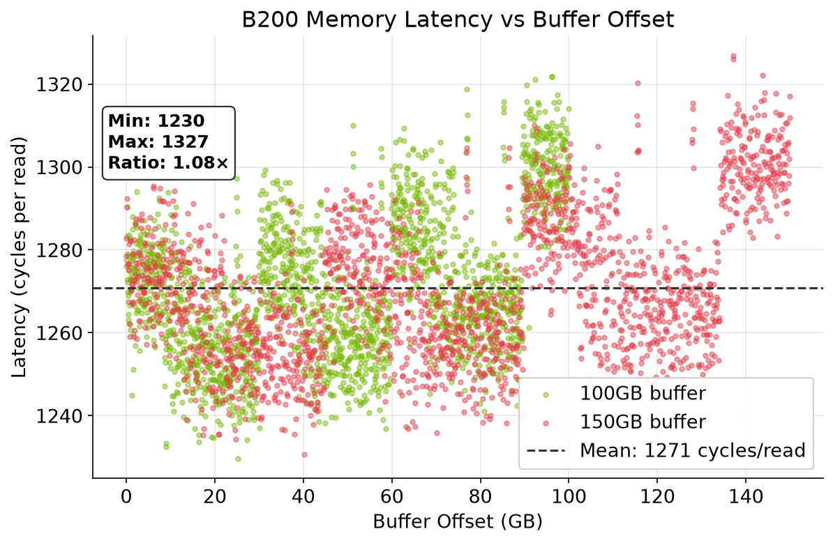
I measured the same question at HBM depth. I created a pointer chase kernel that traversed a 150GB buffer. This is 82% of the total VRAM spanning both dies. Each read’s address depends on the previous read’s value, preventing pipelining or prefetching. Each block ran 2000 dependent reads and recorded total cycles. I divided by 2000 to get per read latency. The result was uniform across all offsets. 1231–1327 cycles per read (1.08× ratio) with no bimodal distribution.
| Buffer Size | Min cycles/read | Max cycles/read | Ratio |
|---|---|---|---|
| 10 GB | 447 | 484 | 1.08x |
| 100 GB | 1,230 | 1,322 | 1.07x |
| 150 GB (spans both dies) | 1,231 | 1,327 | 1.08x |
Recent work using an SM by memory region latency matrix measured an approximately 30 cycle cross die HBM penalty on B200 (link). Against the roughly 1270 cycle HBM latency measured here, 30 cycles is only about 2.4%. That smaller effect could be obscured by normal latency variation and by averaging together accesses whose physical die locality was unknown.
Wrapping Up
Blackwell brings some serious firepower. A fully decoupled Tensor Core with its own memory, 2.25 PFLOPS FP16, 9 PFLOPS FP4 and an interconnect that hides the two die penalty at HBM. But the tradeoffs are real. Tensor Core throughput has grown much faster than SFU throughput, scalar FP32 throughput remains unchanged and the epilogue is where register pressure actually lives. I’ll be working more with the B200 and sharing findings along the way.